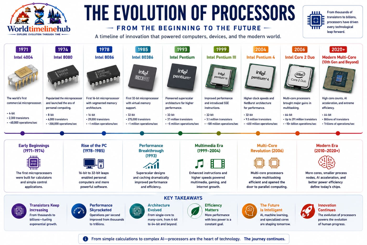
From room-sized vacuum-tube machines to billion-transistor chips in your phone — follow how the CPU became
faster, smaller, multi-core, mobile-first, and AI-ready.
Every app run, video call, and game frame depends on processor innovation. This page maps the proper CPU
timeline from the 1940s through chiplet designs and into experimental quantum and brain-inspired hardware.
A processor is the part of a computer that runs instructions—reading opcodes from memory, performing arithmetic in an ALU, and updating registers. Early machines wired that logic from vacuum tubes; today a single chip holds billions of transistors, multiple cores, caches, and specialized AI units.
The sections below trace that path from ENIAC and the transistor through the microprocessor, PC wars, mobile SoCs, chiplets, and experimental quantum and neuromorphic hardware—with tables for key events, Intel generations, process nodes, and pioneers.
Big picture
CPU evolution in one view
Processors execute instructions—fetch, decode, execute, store. Each era shrank the switching device
(tube → transistor → IC → single chip), raised clock speeds, added cores and caches, then specialized
units for graphics and neural networks. The stats below anchor that story to ENIAC, the first commercial microprocessor, and today’s AI-capable silicon.
CPU evolution: from room-sized tube machines to billion-transistor chips with cores, caches, and NPUs.
💡 Electronic Brains1940s
Vacuum Tube Processors
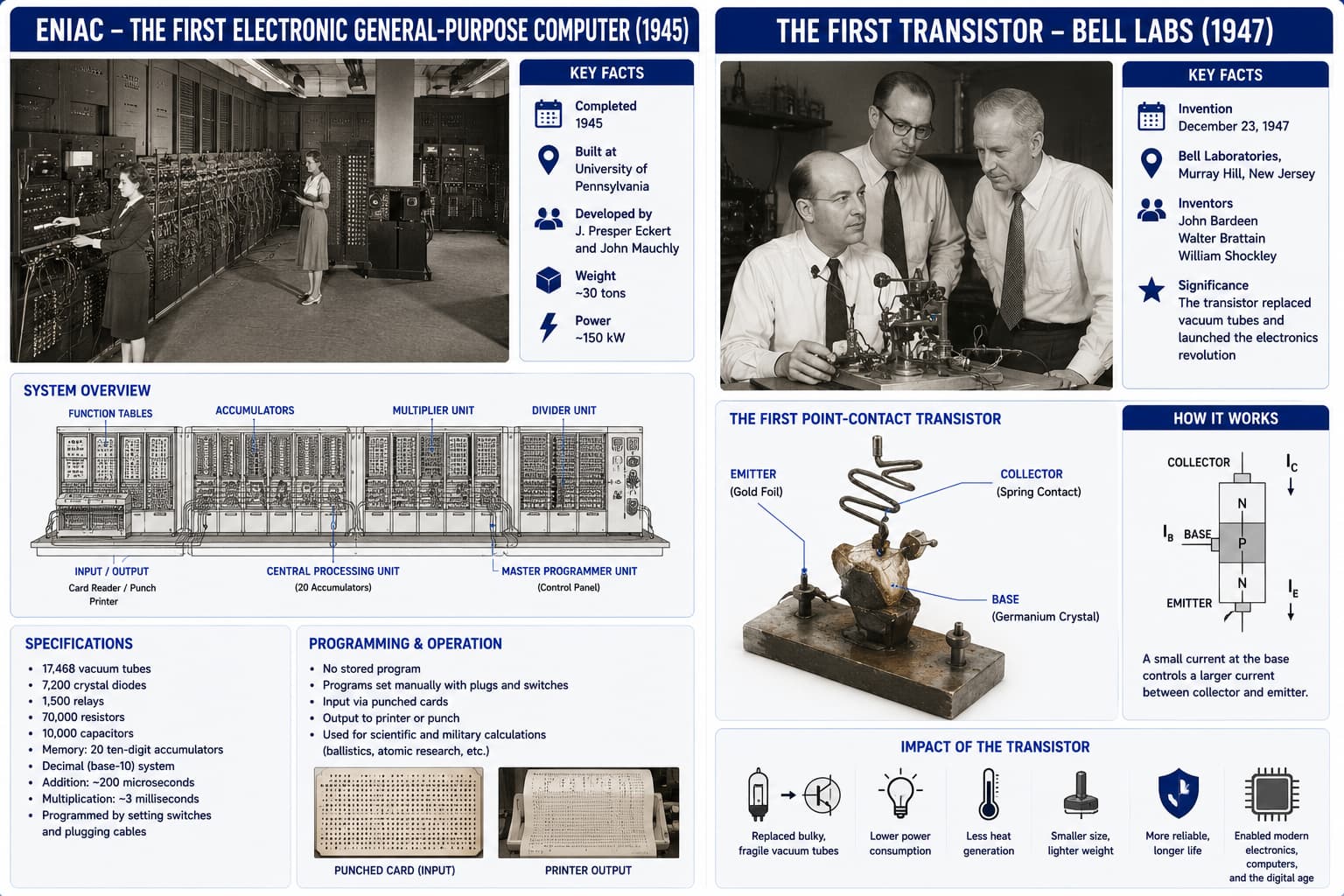
Before silicon, electronic computers used glowing vacuum tubes as switches. Room-sized machines like ENIAC proved that programmable calculation could replace human “computers” with slide rules—but heat, power, and burned-out tubes pushed engineers toward solid-state designs.
Vacuum tube era computing gave way to transistors—smaller, cooler switches that made stored-program mainframes practical.
1945: ENIAC (Electronic Numerical Integrator and Computer) begins operation at the University of Pennsylvania.
1943–45: Colossus in the UK breaks coded messages using tube-based logic.
Programs set by plugs and switches — reprogramming takes days.
Technology Used
Vacuum tubes (valves): Glass bulbs amplify or switch electrical signals.
Decimal or binary logic: Arithmetic built from adders and flip-flop circuits.
Mercury delay lines / punch cards: Early memory and input methods.
How Processing Works
Switching with heat: Tubes turn current on or off; thousands wired together form gates (AND, OR, NOT).
Sequential steps: Clock pulses advance the machine through add, compare, and branch operations encoded in wiring.
No single chip: “CPU” is a room of racks — the program is the physical configuration.
Slow reliability: Tubes burn out often; technicians hunt failed bulbs while the machine is down.
Features
First general-purpose electronic computing: Ballistics tables and cryptography at unprecedented speed.
Huge power draw: ENIAC consumes roughly 150 kW.
Foundation for stored-program idea: Leads to EDVAC and modern architecture concepts.
🔌 Solid-State Switch1950s
Transistor Computers
The 1947 transistor let computers shrink and run cooler than tube machines. Mainframes with magnetic core memory and stored programs became the backbone of banks, universities, and government—establishing the von Neumann model of code and data in memory that still defines how CPUs work.
1947: Bell Labs invents the transistor; computers adopt it in the 1950s.
1956: IBM 305 RAMAC and other transistor machines enter commercial use.
Smaller, cooler, and more reliable than vacuum-tube systems.
Magnetic core memory: Tiny ferrite rings store bits with current pulses.
Assembly language: Symbolic programming replaces pure machine wiring.
How Processing Works
Gate-level logic: Transistors wired as gates perform the same Boolean math as tube machines, but faster and smaller.
Stored programs: Instructions sit in memory; the CPU fetches opcodes and data from core memory sequentially.
ALU operations: Adders and shifters inside the CPU execute arithmetic; results written back to core or registers.
Batch processing: Computers run job queues — users submit decks, operators mount tapes between runs.
Features
Commercial viability: Businesses and universities buy transistor mainframes.
Lower maintenance: Fewer catastrophic hardware failures than tube era.
Bridge to ICs: Sets demand for even denser logic on one substrate.
🧩 Many Circuits, One Die1960s
Integrated Circuit (IC) CPUs
Photolithography packed entire logic boards onto a single silicon die. Gordon Moore’s 1965 observation predicted relentless miniaturization; minicomputers put computing on a lab bench instead of only in a shared machine room.
1958–59: Jack Kilby and Robert Noyce develop integrated circuit techniques.
1965: Gordon Moore observes transistor density doubling roughly every two years (Moore’s Law).
SSI then MSI packs dozens to hundreds of gates per chip — minicomputers emerge.
Technology Used
Photolithography on silicon: Etch transistors and wires onto a wafer.
TTL and early MOS logic families: Standard building blocks for board designers.
Minicomputers (PDP-8, etc.): Departments get local machines, not just mainframe time-sharing.
How Processing Works
Chip-level integration: Multiple gates per package reduce wire length and delay between functions.
Register files grow: More fast storage inside the CPU cuts trips to slower core memory.
Instruction sets stabilize: Families like PDP-11 define opcodes software can target for years.
Time-sharing: One CPU switches between users’ programs via interrupts and the OS scheduler.
Features
Cost per function drops: More people access computing power.
Higher clock potential: Shorter signal paths enable faster switching.
Path to one-chip CPU: Entire data path will soon fit on a single die.
📟 CPU on a Chip1970s
Microprocessor
Putting the whole CPU on one chip turned computers into a product anyone could build around. The Intel 4004 and 8080 sparked hobby PCs, embedded controllers, and decades of software written for specific instruction-set families.
Microprocessor era: Intel defined the PC with x86; AMD and others later competed on performance and 64-bit designs.
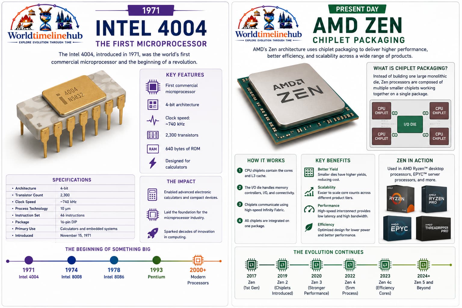
1971: Intel 4004 — 4-bit CPU for a calculator, 2,300 transistors.
1974: Intel 8080 powers early personal computer kits (Altair).
1970s: Motorola 6800, Zilog Z80 compete in embedded and home systems.
Technology Used
Single-die CPU: ALU, registers, and control on one silicon chip.
MOS scaling: NMOS then CMOS improve density and power.
8-bit buses and ISAs: Load/store and stack-based designs for software.
How Processing Works
Fetch-decode-execute loop: Program counter points to next instruction in RAM; control unit decodes opcode and drives the ALU.
External memory: CPU chip talks to separate RAM and ROM chips over address and data buses.
Interrupts: Keyboard or timer signals pause the current program and jump to a handler routine.
Embedded control: Same chip runs washing machines, traffic lights, and the first PCs.
Features
Personal computing born: Hobbyists build affordable kits around 8080/Z80.
Software portability: CP/M and later DOS target specific CPU families.
Industry standardization: Intel architecture influence lasts decades.
🖥️ PC Revolution1980s
16/32-bit PC CPUs
IBM’s choice of Intel for the PC made x86 the default desktop architecture worldwide. Wider registers, protected mode, and early on-chip caches let graphical operating systems and multitasking mature on desks and in offices while ARM quietly began in Acorn’s labs.
1978: Intel 8086 starts the x86 line; IBM PC (1981) uses related 8088.
1985: Intel 80386 — 32-bit addressing and protected mode.
1987: ARM1 designed at Acorn — seeds mobile processor dominance later.
Technology Used
16/32-bit registers and buses: Larger operands and address spaces.
On-chip caches (late 80s): Small SRAM pools hide DRAM latency.
Coprocessors: 8087 math chip accelerates floating-point.
How Processing Works
Protected mode: OS isolates programs with privilege rings — crashes less often kill the whole machine.
Virtual memory: MMU maps program addresses to physical RAM or disk swap space.
Pipelining begins: CPU overlaps fetch and execute stages for higher throughput per clock.
The 1990s superscalar and GHz race made desktops feel instant for browsers, games, and CAD. RISC workstations and AMD competition kept pressure on Intel while MMX and SSE added vector instructions for multimedia and scientific code.
PowerPC, SPARC, and MIPS power Apple, Sun, and SGI workstations.
1999: AMD Athlon competes on performance; 1 GHz barrier approached.
Technology Used
Superscalar pipelines: Multiple instructions per cycle when dependencies allow.
L1/L2 caches grow: Hundreds of KB on-die or on-package.
SIMD extensions (MMX): Vector instructions for multimedia.
How Processing Works
Out-of-order execution: CPU reorders instructions to keep execution units busy while waiting for memory.
Branch prediction: Guesses which way an if-statement goes to avoid pipeline stalls.
RISC vs CISC: x86 decodes complex instructions into micro-ops; RISC machines use simpler fixed-length ops.
OS multitasking: Windows NT, Linux, and macOS run many processes on one CPU via time slices.
Features
Internet-era desktops: Browsers, email, and 3D games demand more MIPS.
Floating-point matters: Science, CAD, and games push FPU performance.
Heat becomes visible: Active heatsinks standard on performance CPUs.
🔀 Parallel Cores2000s
Multi-core x86
When heat stopped easy clock-speed gains, vendors replicated whole CPU cores on one package. Operating systems, compilers, and applications learned to think in threads as 64-bit addressing and hardware virtualization reached servers and desktops alike.
2005: Intel Pentium D and AMD dual-core designs — power limits curb raw GHz gains.
2006: Intel Core 2 Duo improves efficiency per watt.
Quad-core consumer chips arrive late 2000s; servers push 8+ cores.
Technology Used
Multiple cores per package: Shared L2/L3 cache and front-side bus or on-chip memory controller.
64-bit x86-64: AMD64 / Intel 64 extend address space and registers.
Virtualization (VT-x): Hardware assists for running VMs.
How Processing Works
Thread scheduling: OS assigns threads to cores — true parallel execution for independent tasks.
Shared cache coherency: Cores snoop each other’s cache lines so memory stays consistent.
GHz plateau: Performance comes from more cores and wider SIMD, not only higher clock.
Parallel software: Games, video encoders, and servers rewritten for multi-threading.
Features
Better laptop battery life: Lower-voltage cores run when full power not needed.
Data-center scale-out: Blade servers pack many cores per rack unit.
Programming shift: Developers learn locks, races, and parallel APIs.
📱 System on Chip2010s
ARM SoC & Mobile Processors
Phones needed a CPU, GPU, modem, and image processor on one low-power die—ARM licensees delivered. big.LITTLE scheduling matched burst performance with battery life, and billions of devices ran software compiled for ARM rather than x86.
Smartphones use ARM-based SoCs (Apple A-series, Qualcomm Snapdragon, Samsung Exynos).
2010s: big.LITTLE pairs fast and efficient cores on one die.
Tablets and Chromebooks push ARM into laptop territory before Apple Silicon (2020).
Technology Used
SoC integration: CPU, GPU, modem, ISP, and DSP on one chip.
ARM ISA licenses: Companies customize cores (Cortex-A, custom Apple cores).
Thermal budget: Phone SoC throttles when hot — sustained GHz lower than peak burst.
Features
Billions of devices: ARM architecture dominates unit volume worldwide.
Energy efficiency leader: Performance per watt beats desktop x86 in mobile form factors.
App ecosystem: iOS and Android binaries compiled for ARM, not x86.
🤖 AI on Silicon2020s
Chiplets & AI Accelerators
Advanced packaging stitches multiple dies into one processor while NPUs and GPU tensor cores handle neural-network math beside the CPU. Apple M-series and AMD Zen chiplets show that efficiency, AI features, and fab strategy now sell chips as much as peak GHz.
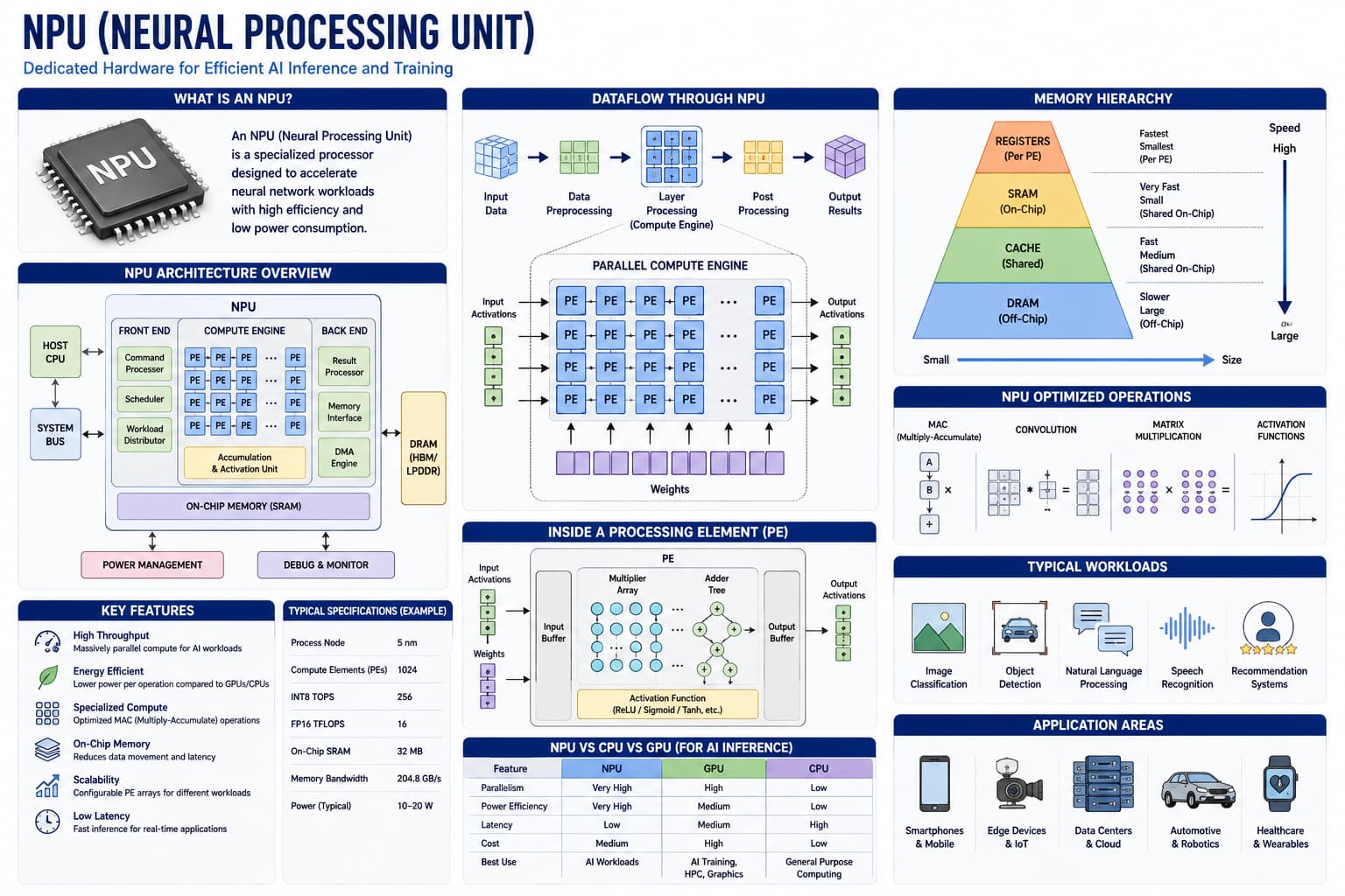
Chiplets and NPUs: specialized silicon runs AI inference while CPU cores handle the operating system and everyday apps.
2020: Apple M1 — ARM SoC replaces Intel in Macs with unified memory.
AMD chiplet designs (Zen 2+) combine multiple CPU dies on one package.
NPUs, TPUs, and GPU tensor cores accelerate machine-learning inference and training.
Technology Used
Chiplet packaging: Infinity Fabric, EMIB, or interposers link dies.
5 nm / 3 nm processes: TSMC and Samsung fabs push density limits.
Dedicated AI engines: Apple Neural Engine, Qualcomm Hexagon, Intel NPU.
How Processing Works
Split workloads: CPU runs OS and general code; NPU/GPU runs matrix math for AI models.
Unified memory: CPU and GPU share one pool — less copying of large model weights.
On-device inference: Voice, camera, and Copilot-style features run locally when possible.
Features
ARM on desktop: Laptops rival x86 on battery and performance per watt.
AI PC category: Marketing pushes NPUs for Windows Copilot+ PCs.
Supply-chain complexity: Advanced fabs concentrated in few regions globally.
🔮 Beyond CMOSFuture
Quantum & Neuromorphic Processors
Quantum and neuromorphic hardware will not replace your laptop CPU soon, but they target specialized problems alongside ever-refined CMOS. Nation-states and cloud giants fund both because cryptography, chemistry simulation, and low-power sensing may depend on computing models beyond classic gates.
Quantum processors (IBM, Google, IonQ) manipulate qubits for specific math problems.
Research on carbon nanotubes, gallium nitride, and 2D materials may extend Moore’s Law.
Technology Used
Superconducting or trapped-ion qubits: Fragile quantum states with error correction.
Memristor crossbars: Analog weights for in-memory computing experiments.
Extreme EUV nodes (2 nm and below): Continued CMOS refinement in parallel.
How Processing Works
Quantum parallelism: Qubits explore probability amplitudes — not faster Excel, but specialized chemistry and crypto research.
Neuromorphic spikes: Events fire between nodes asynchronously; good for sensory pattern recognition at low power.
Hybrid systems: Classical CPU hosts programs that call quantum or neuromorphic coprocessors as accelerators.
Software rewrite: New languages and compilers (Q#, neuromorphic SDKs) unlike x86 assembly.
Features
Niche today, strategic tomorrow: Nation-states and cloud giants fund R&D heavily.
CMOS still mainstream: Phones and PCs remain silicon logic for years ahead.
Ethics and security: Quantum threatens some encryption; policy races engineering.
Proper Processor Technology Timeline
Official era-to-processor mapping for quick reference—each row ties a decade to the dominant silicon style and why it mattered for software, power, and who could afford a machine. Use this table as a map before the detailed events, Intel generations, transistor counts, and comparisons below.
Era
Processor Type
Short Description
1940s
Vacuum Tube Processors
Room-sized machines using glass tubes to switch signals; ENIAC proved electronic, programmable calculation at the cost of heat and constant maintenance.
1950s
Transistor Computers
Solid-state switches replace tubes; magnetic core memory and stored programs make commercial mainframes reliable enough for business and research.
1960s
Integrated Circuit CPUs
Many logic gates on one silicon die; minicomputers spread and Moore’s Law forecasts exponential growth in transistor counts.
1970s
Microprocessor
Entire CPU on one chip (4004, 8080); hobby PCs, embedded control, and software ecosystems target specific instruction-set families.
1980s
16/32-bit PC CPUs
x86 wins the IBM PC clone market; protected mode, caches, and coprocessors support GUIs while ARM is born for low-power systems.
1990s
Pentium & RISC Workstations
Superscalar pipelines, branch prediction, and SIMD; GHz marketing and Windows NT push desktops into the internet age.
2000s
Multi-core x86
Multiple cores per package when GHz gains hit power limits; 64-bit addressing and hardware virtualization reshape servers and PCs.
2010s
ARM SoC & Mobile
Phone SoCs merge CPU, GPU, modem, and sensors; big.LITTLE scheduling balances burst speed with battery life for billions of users.
2020s
Chiplets & AI Accelerators
Multi-die packages and 5 nm/3 nm nodes; NPUs and unified memory make on-device AI practical on laptops and phones.
Future
Quantum & Neuromorphic
Specialized processors for quantum chemistry, optimization, and spiking networks alongside continued CMOS refinement.
Key Processor Historical Events
Beyond the main era cards, these milestones shaped how computers moved from vacuum tubes to microprocessors, multi-core desktops, and ARM SoCs with on-chip AI. Each row highlights a turning point—hardware invention, commercial product, or architecture choice that still influences PCs and phones today.
Event
Year
Significance
ENIAC completed
1945
First general-purpose electronic computer (vacuum tubes)
Transistor invented
1947
Bell Labs — foundation of solid-state computing
First integrated circuit
1958–59
Kilby (TI) and Noyce (Fairchild)
Moore’s Law observation
1965
Gordon Moore predicts transistor density doubling every ~2 years
Landmark “first” achievements in stored-program computing, microprocessors, bit-width, cores, and smartphone AI silicon. When you see a spec sheet advertising 64-bit, dual-core, or an NPU, it traces back to one of these pioneering chips or research machines.
First
Year
Achievement
First stored-program computer
1948
Manchester Baby (SSEM)
First transistor computer
1953
Manchester Transistor Computer
First commercial microprocessor
1971
Intel 4004 (4-bit)
First 8-bit microprocessor
1972
Intel 8008
First 16-bit microprocessor
1978
Intel 8086
First 32-bit microprocessor
1985
Intel 80386
First 64-bit consumer CPU
2003
AMD Athlon 64
First dual-core CPU
2005
Intel Pentium D and AMD Athlon 64 X2
First 1 billion transistor CPU
2007
Intel Itanium 2 (and later Core i7)
First smartphone SoC with NPU
2017
Apple A11 Bionic
Intel x86 CPU Generations (Desktop)
How Intel’s desktop line grew from 16-bit 8086 through Pentium, Core, and hybrid P+E-core designs—with rising transistor counts at each node. Notice how features (protected mode, on-chip cache, integrated memory controller, efficiency cores) arrived in waves rather than all at once.
Generation
Launch Year
Key Features
Transistor Count
8086/8088
1978–79
16-bit, x86 ISA origin
29k
80286
1982
16-bit, protected mode
134k
80386
1985
32-bit, paging
275k
80486
1989
L1 cache, integrated FPU
1.2M
Pentium (P5)
1993
Superscalar, 64-bit data bus
3.1M
Pentium Pro / II / III
1995–99
L2 cache, MMX, SSE
~7–9M
Pentium 4 (NetBurst)
2000
Deep pipeline, high GHz
42M–125M
Core (Core 2 Duo)
2006
Multi-core, 64-bit, efficient
~291M
Core i (Nehalem)
2008
Integrated memory controller
~731M
Core (Skylake)
2015
14 nm, DDR4
~1.75B
Core (Raptor Lake)
2022
Hybrid (P+E cores), DDR5
~5B+
Transistor Count Evolution (Landmark CPUs)
Landmark chips illustrate Moore’s Law in numbers—from thousands of transistors on early microprocessors to tens of billions on modern SoCs. The “factor” column shows growth relative to the 4004 baseline; real-world performance also gained from architecture, not density alone.
Processor
Year
Transistors
Process Node
Moore’s Law Factor
Intel 4004
1971
2,300
10 µm
1×
Intel 8088
1979
29,000
3 µm
~13×
Intel 80386
1985
275,000
1.5 µm
~120×
Intel Pentium
1993
3.1M
800 nm
~1,350×
AMD Athlon
1999
22M
250 nm
~9,600×
Intel Core 2 Duo
2006
291M
65 nm
~126,500×
AMD Ryzen 7 (Zen 2)
2019
3.9B (chiplet)
7 nm
~1.7M×
Apple M1 Max
2021
57B
5 nm
~24.8M×
Note: From 2,300 transistors (1971) to 57 billion (2021) — roughly 25 million times more switching devices in 50 years, closely following Moore’s Law. Smaller process nodes in the table above made that density possible; chip designers still fight heat, memory latency, and power walls at every generation.
Manufacturing Process Node Evolution
Smaller process nodes pack more transistors per square millimeter—driving faster, more efficient CPUs from Intel fabs and TSMC lines alike. Node names (7 nm, 5 nm) are marketing labels as much as physical measurements; density and power still improve generation to generation.
Process Node
Year Introduced
Company
Transistor Density (MTr/mm²)
Example CPU
10 µm
1971
Intel
~0.05
Intel 4004
1.5 µm
1985
Intel
~0.5
Intel 80386
800 nm
1993
Intel
~2
Intel Pentium
130 nm
2001
Intel, TSMC
~5
Intel Pentium III
65 nm
2006
Intel, TSMC
~10
Intel Core 2 Duo
28 nm
2011
TSMC
~30
ARM Cortex-A
14 nm
2014
Intel
~40
Intel 5th–11th gen Core
7 nm
2018
TSMC
~90
AMD Zen 2, Apple A12
5 nm
2020
TSMC
~170
Apple M1, A14
3 nm
2023
TSMC
~290
Apple A17 Pro, M3
Processor Pioneers
Researchers, inventors, and designers whose work on transistors, microprocessors, instruction sets, and chip architectures still shapes every device you use. Hardware breakthroughs and operating-system software evolved together—UNIX and Linux, for example, targeted whatever ISA was winning in the market.
Person/Company
Contribution
John von Neumann
Von Neumann architecture (stored program concept)
William Shockley, John Bardeen, Walter Brattain
Transistor invention (Bell Labs, 1947)
Jack Kilby
Integrated circuit (Texas Instruments, 1958)
Robert Noyce
Integrated circuit (Fairchild), co-founder Intel
Federico Faggin
Intel 4004 designer
Masatoshi Shima
Intel 4004, Z80 designer
Ken Thompson & Dennis Ritchie
UNIX (influenced processor design for OSes)
Linus Torvalds
Linux kernel (optimized for x86, ARM, RISC-V)
Jim Keller
AMD K8, Apple A4, AMD Zen, RISC-V designs
Sophie Wilson
ARM instruction set designer (Acorn)
Then vs Now: Processor Technology
Compare a flagship PC CPU of the late 1970s with a modern desktop chip—same x86 lineage, vastly different clocks, cores, cache, and transistor budgets. Dollar amounts are approximate; the bigger story is how much compute per watt and per dollar improved even as flagship power draw rose for enthusiast parts.
Metric
Then (1970s–80s)
Now (2020s)
Example CPU
Intel 8088 (1979)
Intel Core i9-13900K (2022)
Clock speed
4.77–10 MHz
5–6 GHz (boost)
Transistors
29,000
~5+ billion
Cores
1
8–24 (P+E cores)
Cache
None
~30–36 MB L2/L3
Memory addressable
1 MB
128 GB+
Process node
3 µm
10 nm, 7 nm, 5 nm, 3 nm
Power consumption
~1–5 watts
~65–250 watts (desktop)
Price (flagship)
~$149 (1980)
$600–700 (2024)
CISC vs RISC vs Accelerators
Modern systems rarely use one style alone. Your laptop may run complex x86 instructions on the CPU, ARM-style efficiency in a phone, and thousands of GPU or NPU threads for graphics and AI—each block optimized for a different kind of work.
Style
Examples
Design idea
CISC
Intel x86, AMD x86
Rich instructions; decode to micro-ops inside CPU
RISC
ARM, RISC-V, early MIPS
Simpler, fixed instructions; more registers, compiler-friendly
GPU
NVIDIA CUDA cores, AMD RDNA
Thousands of parallel threads for graphics and ML
NPU / TPU
Apple Neural Engine, Google TPU
Matrix multiply units tuned for neural networks
Speed, Cores, and Power Trends
Raw clock speed was the headline metric for decades, then gave way to cores, cache, SIMD width, and dedicated AI throughput. Power and cooling now cap sustained performance—especially in laptops and phones that throttle when hot.
1940s: ~5,000 operations per second (ENIAC class) — room-scale power, no single-chip CPU.
1970s µP: Hundreds of kHz → low MHz; kilobytes of RAM addressable on early hobby boards.
1990s: 100+ MHz desktops; heat sinks become mandatory as pipelines deepen.
2000s multi-core: 2–4 cores at 2–3 GHz beat chasing 5+ GHz single-core for most real apps.
2010s mobile: ARM SoCs prioritize performance per watt; burst GHz matters less than battery life.
2020s: 8–24+ cores on desktop; AI TOPS and NPU ratings join GHz on marketing spec sheets.
India spotlight
Processors in India’s tech story
India designs software for global chips, assembles phones, and invests in RISC-V and fab policy — while
hundreds of millions of users leapfrogged desktop PCs straight to ARM smartphones. The timeline below shows how imported x86 office machines gave way to mobile-first silicon and today’s semiconductor mission.
1980s
Imported PC CPUs
8086/80286 systems in offices and computer institutes ran software written for Western PCs; processors were imported, not fabricated locally.
2000s
IT services boom
Indian firms optimized databases and enterprise apps for Intel x86 servers worldwide while most silicon still came from US, Taiwan, and Korea fabs.
2010s
Mobile-first ARM
Affordable Android phones brought Qualcomm Snapdragon and MediaTek SoCs to the mass market—many users’ first “computer” was ARM, not x86.
2020s
Design & policy push
India Semiconductor Mission, RISC-V startups, and assembly/test roles in the global supply chain aim to reduce dependence on imported leading-edge chips.
Test Your Knowledge
20 quick questions from the processor timeline—eras, tables, India spotlight, and “How Processing Works” bullets. Click each question to reveal the answer and check what you remember about tubes, Moore’s Law, x86, ARM, chiplets, and NPUs.
Answer: ENIAC.
Answer: The transistor.
Answer: Gordon Moore (Moore’s Law).
Answer: The first commercial microprocessor (4-bit).
Answer: Intel x86 line (8088).
Answer: Arithmetic Logic Unit.
Answer: Superscalar execution (multiple instructions per cycle).
Answer: Power and heat limits made higher clock speeds harder; parallelism scaled performance.
Answer: System on Chip.
Answer: ARM.
Answer: Apple M-series (M1 and later).
Answer: A smaller die combined with others in one processor package.
Answer: Neural network / AI inference (matrix math).
Answer: CPU instruction processing.
Answer: 64 bits.
Answer: Efficient low-power cores.
Answer: Classical bits (0 or 1 only).
Answer: Main RAM (DRAM).
Answer: Instruction set architecture (ISA).
Answer: Smaller switches, more transistors, more cores, specialized AI units, and new paradigms beyond CMOS.
Classroom activity
Students Tasks
Use these 10 prompts for discussion, homework, or presentations. They connect era cards, comparison tables, and future hardware themes on this page.
Jump to any other technology timeline on WorldTimelineHub.
Disclaimer: This content is AI-generated for educational purposes and may contain errors or outdated details. For correct and authoritative information, please refer to official and reliable sources such as government publications, manufacturers, museums, and academic references.